Toyota Prius Gen3 Board
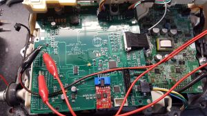
The Toyota Prius Gen3 Board is an open source project to repurpose 2010-2015 Toyota Prius inverters for DIY EV use.
It consists of a open inverter circuit board and programming which replaces the OEM logic board in the prius inverter.
This allows independent control of mg1 power stage, mg2 power stage, buck/boost converter and the dc/dc converter.
*Note that there is also a Toyota Prius Gen2 Inverter for the 2004-2009 model years.
Prius Inverter
The Toyota Prius is a hybrid vehicle. Their inverters are suitable and attractive for DIY EVs because of:
- Large part availability. Priuses (a.k.a. Prii) have been made in large numbers for 20 years.
- High affordability. Prius inverters are available for around $150 from scrapyards
- Durability. Toyota engineers appear to have made the inverters foolproof, many inputs and outputs gracefully handle fault conditions.
- Respectable performance. Rated for 50kW output, but tested to handle 600v, and 500+A on MG2. (MG1 unknown, Gen2 had 70% of MG2 on MG1).
- Ease of repurposing. Emulating the original ECU seems reasonably feasible.
The Gen3 Prius (2010-2015 model years) has a variety of useful components inside the inverter package:
- 2 high power inverters, for the 2 motors MG1 (starter) capable of handling 250 amps, and MG2 (drive motor) capable of handling 350 amps.
- A DC-DC converter to provide 12v power supply to the automotive systems and accessories.
- A boost module to boost the 200v battery pack up to 500v, which looks to be able to function as a battery charger (wish list for future development)
- See this video for a explanation of the How the Prius Gen3 Hybrid Drivetrain Works: https://www.youtube.com/watch?v=PIYNAroYEk0
- See this video for a thorough disassembly and explanation of the Gen2 Inverter and Converter HV System Design: https://www.youtube.com/watch?v=Y7Vm-C4MsW8
- See these videos for a teardown, disassembly and explanation of the Gen3 Inverter: https://www.youtube.com/watch?v=Pw3JqkI6VO4 (Teardown) https://youtu.be/QBoRSXIwZQs (Regarding p0a94 error code for DC-DC Converter Performance)
Control Board
The current version as of Jan 20, 2020 is v2.
As designed by Damien Maguire, the open source hardware for the control board can be purchased from his website:
The control board is a physical replacement for the OEM Prius Gen3 inverter logic board inside the inverter. Remove the old one and replace it with the new one.
Development History
V1 - This board was sold tested but also as a bare logic board requiring purchase of your own components and SMD placement and soldering skills.
V2 - A new board source was found to be both high quality and low cost. The boards were redesigned around the inventory of parts available from this supplier. In particular the high cost of populated and soldered boards (10x the price) from the source used to make the v1 boards is so significantly lower on the v2 that there are likely no savings by building and soldering the board yourself. The circuit now has hardware to support repurposing the MG1 inverter as a battery charger, though as of Jan 20, 2020, software is still in development.
v1c - this board uses mg2 power stage for motor control, and mg1 +buck/boost converter as a battery charger, or parallel connection of MG1 and MG2 to give more amps to a single motor.
v1d - this board allows to use mg1 and mg2 power stages for dual motor control
Vendors
EVBMW Webshop
Support
Community support is available on the Prius Gen 3 Inverter Logic Board Support Thread
You are not entitled to support, purchase from a vendor who offers support if you want it guaranteed. Treat the community with respect.
Inverter Model Numbers
| Inverter No | Car model(s) | Logic Board No | Power Board No | Compatible 50 pin connector | PCB size | Confirmed works with board | Link |
|---|---|---|---|---|---|---|---|
| G9200-33171 | Camry (RHD, unknown year) | ||||||
| G9200-47141 | Auris 2012, Prius 2011 |
F1759-47041 01 | https://openinverter.org/forum/viewtopic.php?t=6895 | ||||
| G9200-47140 | Prius 2010 | F1759-47041 01 | Yes | Yes | |||
| G9200-47162 | Prius + | F1759-47041 01 | F1789-47090 | ||||
| G9200-47180 | Photo diyelectriccar.com | ||||||
| G9200-47190 | Auris 2017 | F1759-47070 05 | F1789-52010 | ? | Forum Thread openinverter.com | ||
| G9200-47210 | Prius 2012 | F1759-47070 05 | YES | 154x143mm | Yes | https://openinverter.org/forum/viewtopic.php?p=16539#p16539 | |
| G9200-47220 | Prius 2014 | F1759-47070 05 | YES | 154x143mm | Yes | https://openinverter.org/forum/viewtopic.php?p=21384#p21384 | |
| G9200-47230 | Prius 2015 | F1789-52010 | Yes | 154x143mm | https://openinverter.org/forum/viewtopic.php?p=29248#p29248 | ||
| G9200-52010 | Yaris
Prius C |
F1759-52010 04 | F1789-52010 | 154x143mm | https://openinverter.org/forum/viewtopic.php?f=14&t=257&p=5828#p5828 | ||
| G9200-52031 | Yaris 2016 | F1759-52010 04 | F1789-52010 | YES | YES | ||
| G9200-52032 | Yaris 2015 | F1759-52010 04 | F1789-52010 | YES | Long 143mm | Forum Thread openinverter.com Forum Thread openinverter.com | |
| G9201-52011 | Yaris | YES | Forum Thread openinverter.com | ||||
| G9201-52012 | Prius C | F1759-52010 | F1789-52010 | YES (presumably) | Forum Thread openinverter.com | ||
| G9200-52030 | Prius C (a.k.a. Prius Aqua) | F1759-52010 04 | F1789-52010 | 154mm long | Forum Thread openinverter.com |
Kit Assembly Instructions (V1C)
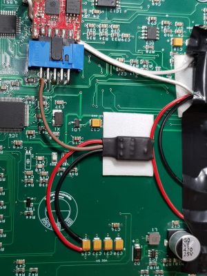
This guide is for the assembly of version V1C of the Gen 3 board available here: https://www.evbmw.com/index.php/evbmw-webshop/toyota-built-and-tested-boards/prius-gen-3-inverter-built-tested
This is based on the assembly videos by Damien Maguire.
Part 1: https://www.youtube.com/watch?v=QE-zym8iIgM&t=2643s
Part 2: https://www.youtube.com/watch?v=Nu5_OBOPk4s&t=1787s
LDO strengthening
The stock 3V3 LDO (3.3V linear voltage regulator) does not provide sufficient current for both the STM32(s) and wifi module(s). Therefor the wifi module needs a distinct regulator.
TODO: does this also affect the latest revision boards?
Early Board Correction, pre July 2020
The first batch of JLCPCB boards shipped have an incorrect resistor value that needs to be changed over. Boards shipped after Jun 26, 2020 will not need to do this.

Resistor labeled R101 (labeled '1002') needs swapping for a 8k2 (0805 package) resistor.
Motor Temperature Sensor correction.
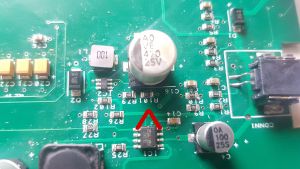
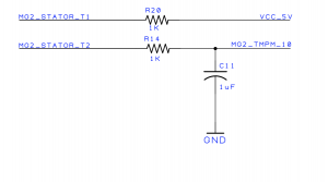
Boards currently have an error with the temperature sensor circuit. R14 is supposed to be in parallel with C11 to form the voltage divider. One workaround would be to put a 1k resistor from one of the pads to ground. this can be done externally if you'd rather not modify the board, put a 1k ohm resistor from MG2_STATOR_T2 to a ground pin. Then connector the temperature sensor from MG2_STATOR_T1 to MG2_STATOR_T2 as normal.
This is a current issue on the boards. A new revision is not yet available.
Wifi Module Correction
The capacitor may need increasing to 10uF deal with noise. The table below shows which boards need updating and which capacitor(s) to update.
| Board Version | Cap(s) needs updating? | Cap(s) to update |
|---|---|---|
| Single motor, large board (v1b) | Maybe | C48 |
| Single motor, small board (v1c) | Maybe | C49 |
| Single motor, small board (v1c, block 3) | Maybe | C49 |
| Dual motor, small board (v1d) | No | N/A |
| Dual motor, large board (v1d) | Maybe | C58 and C86 |
| Dual motor, large board (v1d, block 3) | Maybe | C58 and C86 |
| Dual motor, large board (v1d, block 4) | No | N/A |

DC-DC Startup Delay (V1c & V1d)
These revision boards will start up the DC-DC converter during pre-charge, if you've soldered the jumper. This will mean the current for the DC-DC will be drawn during pre-charge, potentially preventing the main contactor closing.
See https://openinverter.org/forum/viewtopic.php?f=14&t=1039 for more details.
Soldering The Breakout Board
Solder the Ampseal socket to the the breakout board, the silk-screen indicates side and orientation fitment.
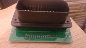
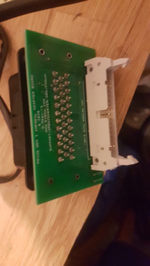
Next flip it over and solder the 34 way IDC locking header on, notch upwards as show.
Note: Some versions of the breakout board have and error in the silk-screen that indicate orientation incorrectly, with the notch towards the bottom.
Soldering the Main Board
The main board is mostly pretty easy to solder, the one exception is the 50 way white connector. I found that putting flux on the pads and dragging solder across them, placing the connector in place and then placing the iron on the pins was the easiest.
Also easiest is to start with this connector, whilst the most complicated, starting with an unpopulated board allows easier access to it as the following connectors are largely around this one.
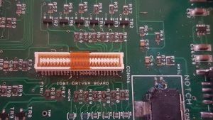
This connector is available on AliExpress https://www.aliexpress.com/item/4001293423321.html if you need additional connectors.
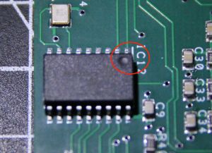
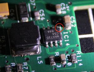
Depending on the kit and time you received it due to chip shortages, you might have IC12 and IC14 unpopulated and need to solder them on.
Each chip's 'pin one' has a small notch to indicate it and this matches the line and IC12 /IC14 silk screen on the board.
Again these are easier to get out of the way before the connectors are positioned.
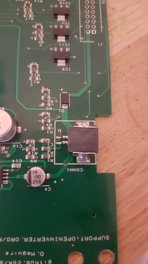
Next up I did conn 1, it can only go one way, and is a piece of cake after the 50 way connector.
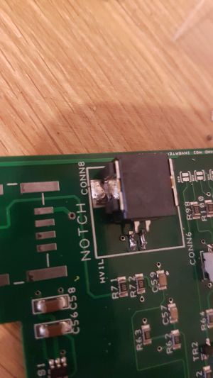
And Conn8, again easy.
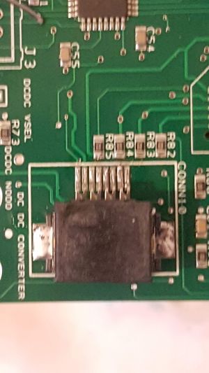
Next the DCDC convert connector, again only fits one way.
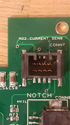
MG1 and MG2 Current sensor Connectors, both these are the same, the tabs on both MG1 and MG2 are at the top.
Ignore the 'Notch' on the board it needs to face outwards to the edge of the board, you'll also need to turn the sensor cables 180 deg to fit when installing the board.
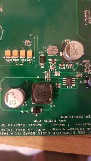
Next up the L2 inductor, it can go either way
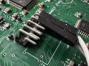
Next up I did the right angled pins for the wifi module, stick the pins in the module connector and then through the board, hold it in place and flip it over.
NOTE: This is how 'not' to mount the right angle connector. The black plastic should be perpendicular to the board and is used to limit the Olimex WifI Board connector.
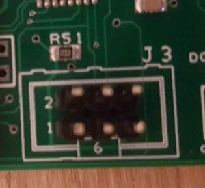
Cut 2 lengths of 3 pins from the header pin strips for the ISP header for programming the Atmega328P that will be used ton control the buck-boost converter.
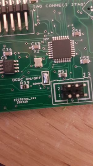
To enable the DCDC converter for I've bridged over the 2 pin holes, but you can add a switch or something here, or leave it open if you're not using the DCDC to keep the 12v battery charged.
See note above for V1C and V1D boards
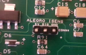
Pin header for Alegro current sensor, currently no software exists to control the buck boost, hopefully in the future this will be able to be used as a charger, this pin header is for the possible addition of a current sensor to facilitate.
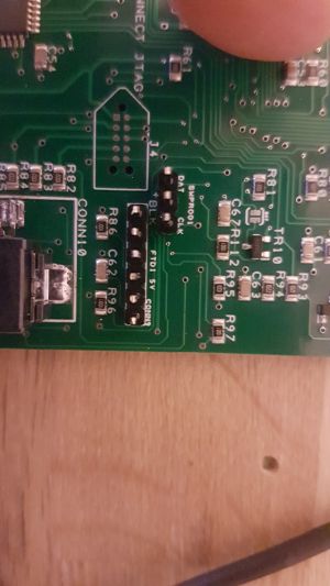
Three options exist on the board for flashing the firmware to the STM32.
If you plan on programming your board with a TC2050 JTAG [1] then obviously skip the next step.
Solder a 3 pin headers for single wire program interface, or a 6 pin header for FTDI interface.
The photo below shows both headers populated, however you don't necessarily need both.
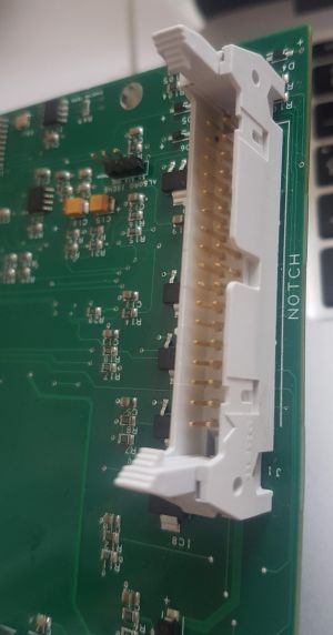
Last up is the 34-way ICD interlock connector for the breakout board. Notch outward.
Powering up
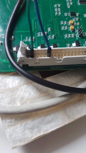
Now it's time to power up the board with 12v and test.
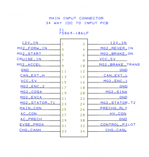
Green wire is +12v (pin 1) and blue 0v (pin 11)
NOTE: When Idle, board consumes about 1.7 - 1.8A of current. When PWM starts, current consumption goes up to ~2A.
Checking voltages
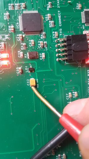
Check for ~3.3v here on C32
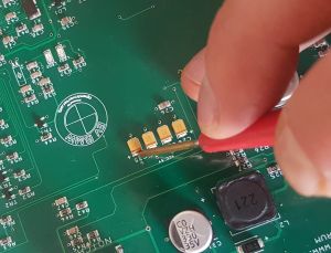
Check for ~5v here on C21/C20/C22/C25
Check for -5v here on the little via next to CONN7 or right next to CONN2 there's a via with -5V under it.
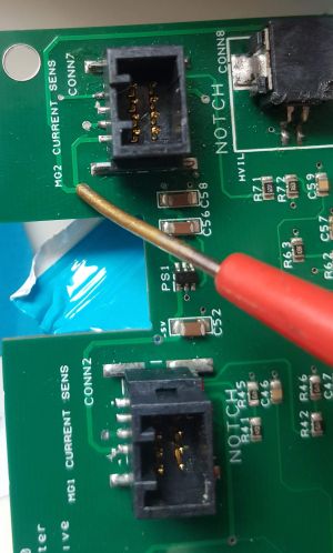
Finally the 26v
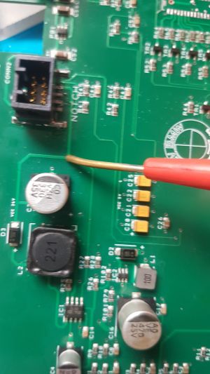
Firmware
Full kits will be supplied programmed and partial kits will be un-programmed.
Wifi Module Firmware
The WiFi module supplied as part of a kit will have the default SSID of inverter and a password of inverter123
My wifi module came with the firmware already installed, but if yours didn't follow the outline steps below. You will need a 3.3v USB to Serial adaptor.
- Download the software from https://github.com/jsphuebner/esp8266-web-interface
- Install the Arduino core from https://github.com/esp8266/Arduino (Arduino IDE, Platform.IO etc supported)
- Write code to ESP8266
- Write filesystem to ESP8266
Step by Step using Arduino IDE
- Add https://arduino.esp8266.com/stable/package_esp8266com_index.json into Additional Board
- Go to Boards -> Board Manager and install ESP8266
- Extract the esp8266-web-interface software to your Arduino projects directory
- Create a new folder named data
- Move all files except FSBrowser.ino to the data folder.
- Choose Olimex MOD-WIFI-ESP8266 as the board
- Upload the code using the Arduino IDE
- Use 'ESP8266 Sketch Data Upload' from the Tools menu, this will upload the files in the data directory to the ESP8266
Programming Firmware
There are three different interfaces that are possible to program the firmware.
Below are instructions for using the single wire programming interface with the USB STLink V2[2].
Connect the 3 wire pin headers to the programming device.
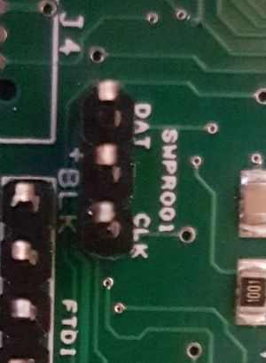
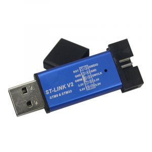
The pin labeled DAT on the board should connect to SWDIO
The middle pin of the 3 pins on the board should go to GND on the STLink V2
The pin labeled CLK on the board should connect to SWCLK
You will also need to hook up power to the board. You can connect the 5V output of the STLink to the 5V pin of the FTDI header. This is the third pin from the left, where pin 1 is just below the letters BLK on the board.
Using a Mac or Linux install https://github.com/stlink-org/stlink
The bootloader can be found here: https://github.com/jsphuebner/tumanako-inverter-fw-bootloader/releases
Run command to write the bootloader
st-flash write stm32_loader.bin 0x08000000
For Windows
Grab the custom bootloader (the .bin file) from https://github.com/jsphuebner/tumanako-inverter-fw-bootloader/releases
Install the ST Link software from here: https://www.st.com/content/st_com/en/products/development-tools/software-development-tools/stm32-software-development-tools/stm32-programmers/stsw-link004.html
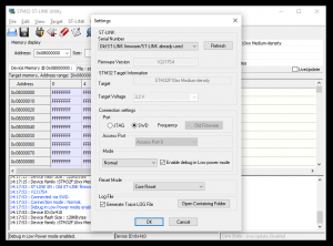
Run the software then select Target>Connect and then Target>Settings to check that your USB device is connected and that the settings look as follows:
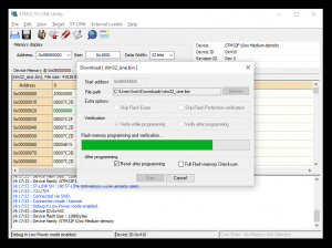
Select File>Open and choose the bootloader from its download location. Then select Target>Program & Verify and you should see this:
Once the bootloader has been programmed the main firmware can be uploaded and upgraded via the web interface.
The main firmware can be found here: https://github.com/jsphuebner/stm32-sine/releases
A wifi network should be visible with the name "inverter" connect to it with password "inverter123"

Once connected open a browser and navigate to http://192.168.4.1 and find the update section, upload the firmware.

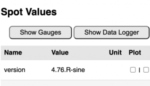
Once this has completed you can verify by scrolling to the Spot Values section and you'll see the software version
Atmega328p Firmware
Be super careful never to program the Atmega while high voltage is applied and caps are not discharged. When cycling through the boot loader, it seems to do something strange that will blow up the otherwise bullet proof buck/boost converter! Also be aware that Arduino also cycles through the boot loader when closing the serial terminal!
This will control the Buck Boost module that's hopefully going to be a functioning charger in the future, it also requires a simple bit of firmware to enable the DC-DC converter.
[Add instructions for firmware]
Inverter Parameters
| Parameter | Suggested Value | Notes |
|---|---|---|
| pwmfrq | 2 | PWM frequency. 0=17.6kHz, 1=8.8kHz, 2=4.4kHz, 3=2.2kHz. Needs PWM restart |
| pwmpol | 0 - Active High | DO NOT PLAY WITH THIS! |
| deadtime | 130 | Deadtime between highside and lowside pulse. 28=800ns, 56=1.5µs. Not always linear, consult STM32 manual. Needs PWM restart |
| il1gain | 4.56 | Digits per A of current sensor L1 |
| il2gain | 4.5 | Digits per A of current sensor L2 |
| udcgain | 5 | Digits per V of DC link |
| udcofs | 0 | DC link 0V offset |
| udclim | 540 | High voltage at which the PWM is shut down |
| snshs | 1 | Heatsink temperature sensor. 0=JCurve, 1=Semikron, 2=MBB600, 3=KTY81, 4=PT1000, 5=NTCK45+2k2, 6=Leaf |
| pinswap | 8 | 0=None, 1=Currents12, 2=SinCos, 4=PWMOutput13, 8=PWMOutput23 |
Parameters Details
First Run (PWM verify)
Once your board in installed in the inverter and all the internal connectors are connected you can power up the inverter with 12v as above. No need to have anything connected to the HV battery or MG1 or MG2. You'll hear an audible wine. We're first going to verify the PWM outputs on the board and then connecting up a motor.
Connect pin 3, MG2_FORW_IN to 12v
Navigate to the Web Interface
Change the parameter encmode to 'AB' as at the moment we don't have any sensors connected.
Set udcmin to 0 to disable precharge.
Set udcsw to 0 so you won't get the Pre-charge fault.
Start the inverter in manual mode with the button

Now set the 2 testing parameters, fslipsnpnt and ampnom to 1.

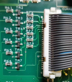
Using a scope, look for a PWM signal on MG2 A/B/C Hi/Low on the 50 pin connector. R74 through R79 can be used as test points for the PWM signal - these are located next to the 50 pin connector as shown in the image below.
Stop the inverter
First Run (Open loop motor spin)
Now connect up the 3 motor phases and a small voltage of around 30v to the HV, I manually pre-charged with a 50w 10ohm resistor for a couple of seconds, the supply needs to be able to supply 10 amps or so. I also had a 20 amp fuse inline.
As above, start the inverter in manual mode, set ampnom to 100 and fslipsnpnt to 10, the motor should start to spin.
You may have Errors to address if this doesn't happen.
DC-DC Converter
The inverter contains a DC DC converter, that is used to keep the 12v battery charged using the high voltage battery. This is the EV equivalent to the alternator on a combustion engined car.
As per the assembly instructions above this needs to be enabled via the jumper on the control board.
In the unmodified state, the DC DC converter will operate with a main battery voltage in the ~80v to ~235v range and will require a simple modification to allow it to operate at higher voltage range, ~140v to ~400v.
There's a couple of options for the DC DC converter. If you aren't planning on using the inverter as a charger and don't want to change the resistors you can use the buck boost module to step down the battery voltage to within the DC DC range.
Unmodified DC DC Resistors, using Buck Boost to step down.
Connect your battery to the inverter as shown below, with pre charge and fuses etc.
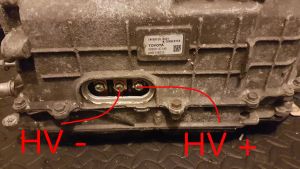
You can use the following sketch on the atmega328p
/*
Runs atmega328p buck/boost control on Prius Gen 3 and Yaris/Auris inverters in buck mode to drop Main HV down for DCDC converter.
Experimental code. Only tested on the bench! Use at your own risk!
D.Maguire
*/
#include <Metro.h>

int HVLow = 0;        // voltage on low side of converter
int HVHi = 0;        // voltage on high side of converter
int SetV = 0;       //set point voltage
int PWMDuty = 0;    //pwm duty cycle

Metro timer_pwm=Metro(5);
Metro timer_serial=Metro(200);

void setup() {
  Serial.begin(9600);//
  TCCR1B = TCCR1B & B11111000 | B00000010;    // set timer 1 divisor to  8 for PWM frequency of  3921.16 Hz
  pinMode(9, OUTPUT); //boost low side
  pinMode(10, OUTPUT); //boost Hi side
  analogWrite(9,0); //low side off
  analogWrite(10,0); //High side off
  SetV=210;  //set at 210v to run dcdc
  PWMDuty=0;


}
// the loop function runs over and over again forever
void loop() {

    HVLow = (analogRead(A0)/1.85)-43; //-43 needed for Lexus CT200h variant. Remove for Prius / Auris.
    HVHi = (analogRead(A1)*1.25);

    updatePWM();  //call pwm update routine.
    serialOUT();  //call serial out routine

}

void serialOUT()
{
  if(timer_serial.check()){
  Serial.print("Low Vbus = ");
  Serial.print(HVLow);
  Serial.print("Volts");
  Serial.print("\t High Vbus = ");
  Serial.print(HVHi);
  Serial.print("Volts");
  Serial.print("\t PWMDUTY = ");
  Serial.println(PWMDuty);
  }
}

void updatePWM()
{
if(timer_pwm.check()){
  if(HVHi>300){  //if hv is above 300v start ramping up pwm and regulate to setpoint.
    if (HVLow<SetV) PWMDuty++;
    if (HVLow>SetV) PWMDuty--;
    if (PWMDuty<0)  PWMDuty=0;
    if (PWMDuty>250)  PWMDuty=250;
    analogWrite(10,PWMDuty);
  }
  if(HVHi<250)
  {
      PWMDuty--;;  //if hv is lower then 250v ramp down pwm
      if (PWMDuty<0)  PWMDuty=0;
  }
}

}
Modified DC DC Resistors, using Buck Boost to bridge.
You must have modified the resistors in the inverter for this method to work.
Connect your battery to the inverter as shown below, with pre charge and fuses etc.

The following sketch can use used on the atmega328p to internally bridge the buck boost module so that the full battery voltage reaches the DC DC converter.
// I/O-PINS
const uint8_t boostLoDrivePIN = 9; // D9 (PB1)
const uint8_t boostHiDrivePIN = 10; // D10 (PB2)


/********
* SETUP *
********/
void setup()
{
  pinMode(boostHiDrivePIN, OUTPUT);
  digitalWrite(boostHiDrivePIN, HIGH); // To set high drive ON

  pinMode(boostLoDrivePIN, OUTPUT);
  digitalWrite(boostLoDrivePIN, LOW); // To set low drive OFF
}


/*******
* LOOP *
*******/
void loop()
{

}
Modified DC DC Resistors and using Buck Boost for charging.
Your battery will be connected to Charging HV + and HV - with contactors and precharge. You will also have another contactor that the atmega328p will control to externally bridge Charging HV+ and Driving HV+ this will externally bridge both sides of the buck boost module when in run mode so that the driving isn't limited by the buck boost module but during charging the contactor will open and the connection is severed.
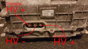
The charing code for the atmega328p is here https://github.com/celeron55/prius3charger_buck, more details on charging is further down in the wiki.
Modifying the DC DC converter resistors
The DC DC converter in unmodified state will startup at a little over 100v and shut down at around 240v, to use it with a higher voltage it needs to be modified by changing some smd resistors.
See https://www.youtube.com/watch?v=Nu5_OBOPk4s&t=2s
You'll need to remove the bottom cover of the inverter to expose the DC DC converter control board.
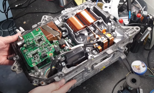
We need to replace 4 resistors on the top side of the board, these are R629, R627, R625, R623, currently 120k ohm, these will need replacing with 210k ohm
(1%, 0.5W, 0805, Manufacturer part#: ERJP06F2103V Farnell #: 2326773 )
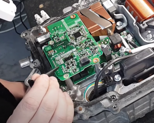
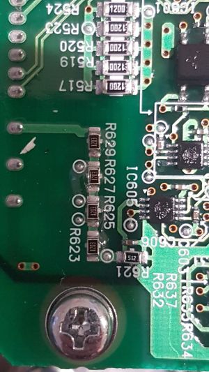
These are the 4 resistors on the top.
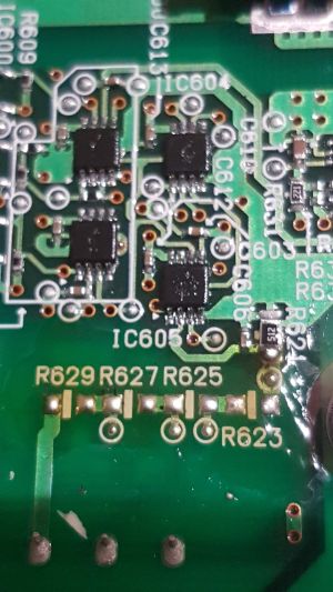
And Replace
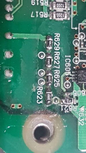
There's also 4 resistors to replace on the bottom, these are R630, R628, R626, R624, these also need to be 210k ohm.
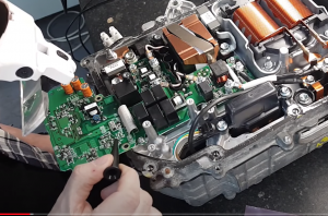

The bottom resistors are up next to the flexible cable, on the underside of the board, to access them, unscrew the 4 screws holding the board in place, unplug the black connector carefully lift the board upwards.
Bare in mind the flexible cable is still attached and is soldered directly to the board. Flip it over.
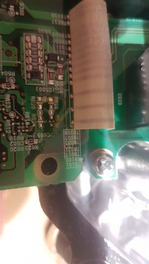
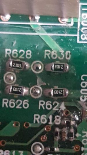
Bottom side replaced. You can now place the board back in place, screw the 4 screws in and don't forget the black plug.
Replace the bottom metal cover.
12v Battery Connection
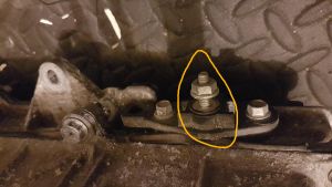
The 12v battery positive connects to this post, it'll output ~14v when the DC-DC is running to keep the battery charged, the negative terminal of the battery should be connected to the case of the inverter.
High Voltage Battery Connection
The HV battery connection is below, DO NOT directly connect the battery here. It needs to be connected via contactors and a pre-charge resistor. This connection point by-passes the buck/boost converter.

[Add details of pre-charge and contactor]
Motor Connection
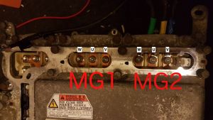
If you are only using MG2 to power a motor, and not paralleling MG1 and MG2, connect your 3 phase wires from the motor to the outer 3 terminals.
Some versions of this inverter have the U-V-W labels for the three phase wires stamped into the case and some do not. These are shown below in case you have a version of the inverter without them and need to connect to a motor other than the originial prius transaxle.
Parallel MG1 and MG2 on a single motor
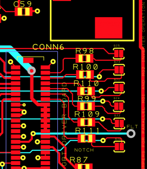
MG1 and MG2 can be used in parallel for more power, to do so there's some solder jumpers on the board to use. Jumpers SJ1 to SJ6 need soldering across the little gap between them.
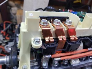
You then need to connect MG1 phase 1 to MG2 phase 1 and so on. This needs to be done before the the current sensors so that all the current goes through MG2 current sensors on the phase bars, otherwise the software cannot measure the current correctly.
IDC Connector
If you are not using the AMPSeal daughterboard, you can connect directly to the 34 pin IDC connector on the EVBMW board.
Connections are as follows:
| Pin Number | Label | Description |
| 1 | 12V_IN | Provide with +12V supply from battery or power supply for testing |
| 2 | 12V_IN | Provide with +12V supply from battery or power supply for testing |
| 3 | MG2_FORW_IN | Active high signal at 12V (switches at >7V) to tell the inverter which way to spin the motor. Take positive feed from 12V battery or supply and wire through a three position switch, with the switched connections running to forward and reverse. |
| 4 | MG2_REVER_IN | Active high signal at 12V (switches at >7V) to tell the inverter which way to spin the motor. Take positive feed from 12V battery or supply and wire through a three position switch, with the switched connections running to forward and reverse. |
| 5 | MG2_START | Active high signal at 12V (switches at >7V) to start the inverter and move it from pre-charge to run mode. Typically connected to the momentary 'START' position of your ignition switch. |
| 6 | MG2_BRAKE_ON | Active high signal at 12V (switches at >7V) to inform the inverter that the car is under braking. Typically takes a feed from the brake switch that also turns on brake lights etc. |
| 7 | CRUISE_IN | Active high signal at 12V (switches at >7V) to turn on cruise control mode. This sets the current motor speed as the set point for cruise control. Cruise control is disabled by a signal from the brake switch. |
| 8 | VCC_5V | +5V supply for temperature and throttle sensors |
| 9 | MG2_ACCEL | 5V analogue input from first channel of throttle sensor. These typically take a 5V supply and ground and return to this pin a variable voltage that indicates throttle position. |
| 10 | MG2_BRAKE_TRANS | 5V analogue input from second channel of throttle sensor. These typically take a 5V supply and ground and return to this pin a variable voltage that indicates throttle position. |
| 11 | GND | Common ground for 12V supply or 5V return. |
| 12 | GND | Common ground for 12V supply or 5V return |
| 13 | CAN_EXT_H | CANBus digital communication connection for remote interface with inverter |
| 14 | CAN_EXT_L | CANBus digital communication connection for remote interface with inverter |
| 15 | VCC_5V | +5V supply for temperature and throttle sensors |
| 16 | MG2_ENC_1 | Can be either digital input for encoder (in which case, connect the relevant encoder output here and provide the device with 5V and ground), or one of the two connections for the SIN winding if you are using a resolver for motor position. |
| 17 | MG2_ENC_2 | Can be either digital input for encoder (in which case, connect the relevant encoder output here and provide the device with 5V and ground), or one of the two connections for the COS winding if you are using a resolver for motor position. |
| 18 | GND | Common ground for 12V supply or 5V return |
| 19 | MG2_COSA | Connect SIN winding of motor resolver here and to Encoder Channel A |
| 20 | MG2_SINA | Connect COS winding of motor resolver here and to Encoder Channel B |
| 21 | MG2_EXCA | Connect exciter winding of motor resolver here and to ground |
| 22 | GND | Common ground for 12V supply or 5V return |
| 23 | MG2_STATOR_T1 | 5V output for the motor temperature sensor. These are typically variable resistance devices. Connect one side of the sensor here. |
| 24 | MG2_STATOR_T2 | Input from motor temperature sensor. Connect the other side of the sensor here. (Note the board correction above. Do not connect if it hasn't been addressed by a new revision or work around) |
| 25 | MAIN_CON | Open Collector (Will switch the ground side from disconnected to ground).
Connect one side of the contactor coil to +12v and the other to this pin. Your contactor will need either a built in economiser or additional circuit. MAX 2 amp. |
| 26 | PRECHG_RLY | Open Collector (Will switch the ground side from disconnected to ground).
Connect one side of the contactor coil to +12v and the other to this pin. Your contactor will need either a built in economiser or additional circuit. MAX 2 amp. |
| 27 | AC_CON | Open Collector (Will switch the ground side from disconnected to ground).
Connect one side of the contactor coil to +12v and the other to this pin. Your contactor will need either a built in economiser or additional circuit. MAX 2 amp. |
| 28 | HV_CON | ? |
| 29 | AC_PRECH | Open Collector (Will switch the ground side from disconnected to ground).
Connect one side of the contactor coil to +12v and the other to this pin. Your contactor will need either a built in economiser or additional circuit. MAX 2 amp. |
| 30 | GND | Common ground for 12V supply or 5V return |
| 31 | EVSE_PROX | |
| 32 | CONTROL_PILOT | |
| 33 | CHG_CANH | CANBus digital communication connection for remote interface with charger |
| 34 | CHG_CANL | CANBus digital communication connection for remote interface with charger |
Ampseal Socket & Plug
There are multiple part numbers for the large 35 way Ampseal through hole socket, with small mating differences, be sure to get a matching pair.
TE connectivity 776164-1 (female) and 776163-1 / 776231-1 are a matched pairs[3]. 776231-1 is the vertical header he uses in the video.
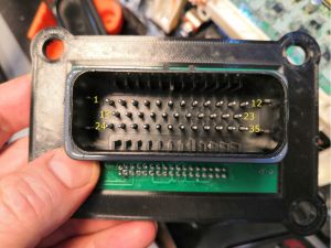
The AMPSeal connector is wired as follows:
| Pin Number | AMPSeal Pinout Label | Description |
| 1 | 12V SUPPLY POSITIVE | Provide with +12V supply from battery or power supply for testing |
| 2 | GROUND | Common ground for 12V supply or 5V return |
| 3 | FORWARD DIRECTION SIGNAL | Active high signal at 12V (switches at >7V) to tell the inverter which way to spin the motor. Take positive feed from 12V battery or supply and wire through a three position switch, with the switched connections running to forward and reverse. |
| 4 | REVERSE DIRECTION SIGNAL | Active high signal at 12V (switches at >7V) to tell the inverter which way to spin the motor. Take positive feed from 12V battery or supply and wire through a three position switch, with the switched connections running to forward and reverse. |
| 5 | START SIGNAL | Active high signal at 12V (switches at >7V) to start the inverter and move it from pre-charge to run mode. Typically connected to the momentary 'START' position of your ignition switch. |
| 6 | BRAKE DIGITAL SIGNAL | Active high signal at 12V (switches at >7V) to inform the inverter that the car is under braking. Typically takes a feed from the brake switch that also turns on brake lights etc. |
| 7 | CRUISE CONTROL SIGNAL | Active high signal at 12V (switches at >7V) to turn on cruise control mode. This sets the current motor speed as the set point for cruise control. Cruise control is disabled by a signal from the brake switch. |
| 8 | 5V OUT | +5V supply for temperature and throttle sensors |
| 9 | ACCELERATOR CHAN 1 INPUT | 5V analogue input from first channel of throttle sensor. These typically take a 5V supply and ground and return to this pin a variable voltage that indicates throttle position. |
| 10 | ACCELERATOR CHAN 2 INPUT | 5V analogue input from second channel of throttle sensor. These typically take a 5V supply and ground and return to this pin a variable voltage that indicates throttle position. |
| 11 | GROUND | Common ground for 12V supply or 5V return. |
| 12 | INVERTER CAN HIGH | CANBus digital communication connection for remote interface with inverter |
| 13 | INVERTER CAN LOW | CANBus digital communication connection for remote interface with inverter |
| 14 | +5V OUT | +5V supply for temperature and throttle sensors |
| 15 | ENCODER CHAN A | Can be either digital input for encoder (in which case, connect the relevant encoder output here and provide the device with 5V and ground), or one of the two connections for the SIN winding if you are using a resolver for motor position. |
| 16 | ENCODER CHAN B | Can be either digital input for encoder (in which case, connect the relevant encoder output here and provide the device with 5V and ground), or one of the two connections for the COS winding if you are using a resolver for motor position. |
| 17 | GROUND | Common ground for 12V supply or 5V return |
| 18 | RESOLVER SIN | Connect SIN winding of motor resolver here and to Encoder Channel A |
| 19 | RESOLVER COS | Connect COS winding of motor resolver here and to Encoder Channel B |
| 20 | RESOLVER EXC | Connect exciter winding of motor resolver here and to ground |
| 21 | GROUND | Common ground for 12V supply or 5V return |
| 22 | MOTOR TEMP SENSOR T1 | 5V output for the motor temperature sensor. These are typically variable resistance devices. Connect one side of the sensor here. |
| 23 | MOTOR TEMP SENSOR T2 | Input from motor temperature sensor. Connect the other side of the sensor here. (Note the board correction above. Do not connect if it hasn't been addressed by a new revision or work around) |
| 24 | MAIN HV CONTACTOR | Open Collector (Will switch the ground side from disconnected to ground).
Connect one side of the contactor coil to +12v and the other to this pin. Your contactor will need either a built in economiser or additional circuit. MAX 5 amp. |
| 25 | HV PRECHARGE RELAY | Open Collector (Will switch the ground side from disconnected to ground).
Connect one side of the contactor coil to +12v and the other to this pin. Your contactor will need either a built in economiser or additional circuit. MAX 5 amp. |
| 26 | CHARGER AC INPUT RELAY | Open Collector (Will switch the ground side from disconnected to ground).
Connect one side of the contactor coil to +12v and the other to this pin. Your contactor will need either a built in economiser or additional circuit. MAX 5 amp. |
| 27 | CHARGER HV DC REQUEST | |
| 28 | CHARGER AC PRECHARGE RELAY | Open Collector (Will switch the ground side from disconnected to ground).
Connect one side of the contactor coil to +12v and the other to this pin. Your contactor will need either a built in economiser or additional circuit. MAX 5 amp. |
| 29 | GROUND | Common ground for 12V supply or 5V return |
| 30 | EVSE PROXIMITY SIGNAL | |
| 31 | EVSE CONTROL PILOT SIGNAL | |
| 32 | CHARGER CAN HIGH | CANBus digital communication connection for remote interface with charger |
| 33 | CHARGER CAN LOW | CANBus digital communication connection for remote interface with charger |
| 34 | NOT USED | |
| 35 | NOT USED |
Connecting Resolver
For resolver connect EXC to one side of the exciter winding and other to Ground.
Connect one side of SIN winding to SIN and other to Encoder A
Conenct one side of COS winding to COS and other to encoder B.
Inverter as charger
The buck/boost module in the inverter can be used to step up or down an input voltage to charge the high voltage battery in the car. Stepping down to a lower voltage is buck and up is boost converting.
Buck Mode Charging.
This is what you need if your battery voltage will be lower than the rectified input (< 340v for 240v single phase, 600v for 3 phase)
There's some firmware for the Atmega on the EVBMW board to control the buck/boost in buck mode for charging.
https://github.com/celeron55/prius3charger_buck
Once you've downloaded the code there's some things to change.
#define BATTERY_CHARGE_VOLTAGE 300 //Set this to your battery full voltage
#define AC_PRECHARGE_MINIMUM_VOLTAGE 550 // European 3-phase rectifies to 600V, Single Phase 240v rectifies to 340V
#define PRECHARGE_BOOST_ENABLED true. // The capacitor needs pre-charging, there's 2 options, a pre-charge resistor on the A.C input or use the battery to boost to the input voltage.
#define PRECHARGE_BOOST_VOLTAGE 550 // European 3-phase rectifies to 600V, Single Phase 240v rectifies to 340V
The battery connection needs to be a little different. The battery + will need connecting to the left most terminal and a contactor will be needed to bridge the left most and right most when running.

3D Printed Parts
 |
 |
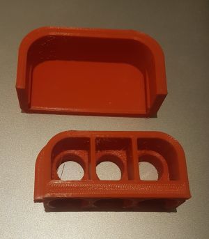 |
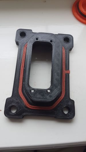
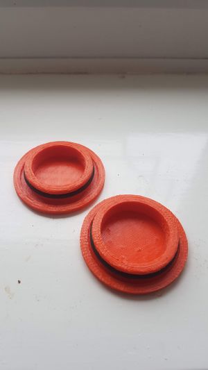
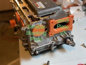
User bobby_come_lately has created a fair few 3D printable parts for use with the inverter. They can be downloaded https://github.com/jamiejones85/Gen3PriusInverter3DParts
More information on these parts can be found in this forum post https://openinverter.org/forum/viewtopic.php?t=836
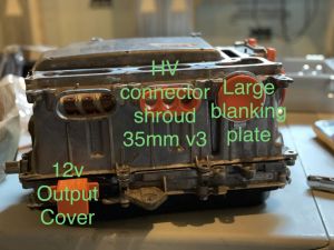
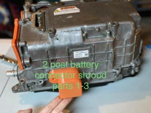
3D Printed Part Locations
Frequently Asked Questions
What happens when the inverter has an ERROR?
The Toyota driver error signals are connected to the pk_in pin on the stm32 so when the Inverter has an error it stops the PWM by giving the STM32 an interrupt signal. See Here
Notes
Bill of Hand Placed Parts (Github)
Bill of Materials (Github)
The control board takes advantage of the OpenInverter.org software for control.
- ↑ https://www.tag-connect.com/product/tc2050-idc-nl-050 (Backup: Web Archive)
- ↑ https://www.st.com/en/development-tools/st-link-v2.html (Backup: Web Archive)
- ↑ https://www.ebay.co.uk/itm/Connector-ECU-Terminals-35P-35-Way-776164-1-776231-1-776163-1-Male-Female-Pins/401764868163?hash=item5d8b0d6043:g:3TkAAOSwexhc1Tcy (Backup: Web Archive)