Nissan Leaf Gen 3 (2018 up EM57)
If you scanned the QR code on your gen 3 Leaf adapter board you are in the right place to help set it up!
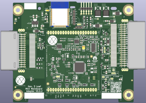
110kw / 160kW
The third generation Nissan leaf stack has both 110kW and 160kW versions. Current understanding is the only difference between these 2 is the Nissan controller board. https://openinverter.org/forum/viewtopic.php?p=45803#p45803
This Open Inverter adapter board replaces the Nissan controller in these gen. 3 inverters. Theory is that either inverter could make at least 160kW with this OI adapter & controller boards if the rest of the system can support it.
This adapter board is compatible with Gen 3 Nissan Leaf (model year 2018-2022?) inverters and the open inverter mini main board
This is a work in progress. This board is not yet tested.
Any deeper dive info is in italics. You can skip over anything in italics if you don't want to know how it works or what it's doing in the background.
Things to verify
Some of the info was not completely clear for the development of this board. Things that need to be verified:
- Let's use
strikethroughas we verify these items. - The board address needs to be checked with the brake circuit connected and disconnected (cut SJ4 to disconnect, solder to connect it.) Need to verify this does not skew the address voltage and change the address. There are vias to measure the voltage in the board address block to help.
- Verify different 32 & 40 position connector footprints match up. Through hole footprints are unknown.
The SMD connectors work properly. The second part of the brake circuit looks like it should block 2.5v and below from turning on the brake lights. Above about 2.7v the brake lights should go on. This depends on if the STM32 can push enough power to overcome a few components. Trying to give a wider range of available addresses and still have the brake light output trigger in regen. The high side switch turns on at around 1.2v on the enable line, that's what the zener blocking diode is for.R3 and R9 are setup as 0R (jumper) resistors. Nissan has 2 lines for each current sensor signal. These should not be populated for now.R2 & R4 are unclear if they should be grounds and are 0R resistor / jumpers. Need to figure out if these are in fact required grounds.J1 connector (Nissan 32 pos.) on position 20 if using thru hole board to wire connectors it only has a .3mm trace to ground which likely won't last or work well. If this ground is required there is a large ground via right next to position 20 to solder to for a good ground connection. Will need to correct this in the next version once understood.
- R13 is a pull down resistor for the T_SINK input.
This is at 3K3 in V0.0.1 but unsure if this is ideal.V0.0.4 changed this to a 1.2k pull down resistor. There are 2 plated thru holes on each side of R13 to use to make testing the ideal value easier. L2 in rev V0.0.2 had an 0805 inductor rated for only 15ma. Changed to a Sunlord 4030 / AKA 4.0mm X 4.0mm inductor that can pass 700ma +. I don't think any V0.0.2 boards were made yet but not sure.- What connector options to use for the Open Inverter connections to get out of the inverter.
The capacitors on each contactor mosfet gate should be checked that they do not delay turn on or off too much and that they help eliminate chatter. If they are too large they could run the mosfets in the linear region and could cause damage.Set these to do not populate, not tested.
There are optional jumpers on both the adapter board and the mini mainboard.
Setting up the mini mainboard jumpers
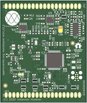
See, Mini Mainboard for details.
SJ1
Mini mainboard back jumper should be **soldered / not soldered.**
This enables a 500 ohm pull-up resistor that is needed for open collector encoders. In the case of the EM57 motor it **is / is not required**.
SJ3
The Mini Mainboard has this soldered / jumpered to the left. It's setup for a cruise control 12v input. It should stay like this.
Soldered to the right is 3.3v MOSI for SPI communications. Do not apply 12v to this input while shorted to the right of the jumper or damage likely will result.
Setting up the 3rd generation Leaf adapter board jumpers

SJ4
Can be ignored. It should stay shorted.
This jumper allows disconnecting the brake output circuitry from the board address circuitry for testing (see Mini Mainboard Hardware Detection.) **add link** This IO is shared between a board address analog input and a brake light output. Once this is proven out there should be no need to change this jumper.
SJ5
Open Inverter has an Emergency Stop (E-Stop) function to quickly, non-destructively, and safely shut down the inverter. To use the E-Stop option, connect an E-stop switch (closed when OK, open in stop position) that feeds 12v to position 40 of this adapter board. The E-Stop switch must break the 12v signal of the circuit when the e-stop is pressed or if a wire breaks. Other methods are not recommended for safety. This is to guarantee it shuts the inverter down when needed. Starting with V0.0.4 pin 26 of the 40 position connector has a solder jumper to 12v. This allows the user to connect on board +12V to pin 26 to be used as the +12V supply for the E-Stop Switch. See p26 +12V below.
You must either feed in 12v on pos. 40 or solder SJ5 closed to feed12v into this E_STOP input or the inverter will not run.
To bypass the E-Stop functionality, solder the SJ5 jumper closed. No need to populate position 40 (e-stop signal) in this bypassed case.
SJ6
Is optional and can be left with both positions open. Never short all 3!
Position 19 on the 40 position Nissan connector is a PWM_USER / OUT_TEMP signal. Part of the PWM_USER circuitry is an optional 0805) pull up resistor (R19) that is not populated. An 0805 SMD resistor can be added if a pullup is desired on board (the footprint is for a hand solder 0805, it's larger than normal but makes it easier to modify and hand solder.) SJ6 is a voltage select solder jumper to select between the onboard voltages of 5.3V and 12v to create the wave form / signal on this output. There is also a plated through hole labeled as UV1 (user voltage) that can be used for the pull up with a a different voltage if desired. Do not solder / short SJ6 if UV1 is used.
C11 capacitor is to reduce EMI. If your PWM device needs a very sharp edge this may interfere. C12 is a 1uF capacitor to help stabilize the user selected voltage, covers 5.3, 12v and user voltage selections. To the left of this +12V pad is a plated through hole to supply an unregulated +12v to be used for a user supplied voltage regulator for a different voltage. The n channel mosfet is rated for 100v and 1.5 amps. This is a common footprint with a wide range of voltages and currents up to about 1.5 amps.
SJ8 / J8
Are voltage select jumpers. SJ8 is a solder jumper and J8 is a 3 position male pin header. You must use only one style jumper to select 3.3v or 5v for your programmer so you do not accidently short 5.3v and 3.3v together. J8 has 2.54mm / .1 inch pin spacing, common jumper caps will work to select the voltage. See programming the ESP32 below for further info on programming.
SJH1 & SJL1
These should be either both soldered if a 120ohm CAN termination resistor is desired here. If this is the end of a CAN line these should both be soldered. CAN lines should be terminated at each end of the lines with a 120 ohm resistor. Do not leave one solder jumper open & one closed.
There is a capacitor in the middle of the 2x 60 ohm resistors to help filter noise on the CAN lines. There is also a TVS diode (D6) right next to the 40pos. connector to help with static protection.
p26 +12V
On the 40 position connector there is a solder jumper on the back of the board. This is meant to supply +12V to pin 26 of the 40 position Nissan connector to be used for the E-Stop function if desired (connected to both the SMD and through hole footprints.) There are very thin traces from the solder jumper up to a +12v plated through hole above the MOSI label meant to act as a crude fuse.
IL1 & IL2
Il1 & IL2 are redundant current sensor signal paths. OEMs commonly use 2 signal paths for each current sensor to the inverter controller. Open inverter uses 1 trace for each current sensor, these solder jumpers can be soldered closed to switch to have 2 signal paths to the inverter brain. These can both be left open.
OI Automatic Mini Maniboard Address Detection
Automatic board detection was introduced with this board in combination of the Mini Mainboard. Mini Mainboard#Hardware detection There is nothing to do here, the Open Inverter environment should automatically detect which board this is and populate settings for it. This sense line is shared with the brake output, see the "Brake Output section at the bottom for more info.
Soldering on the Nissan header connectors
The adapter board is setup with multiple footprints for both of the 32 and 40 position inverter's internal Nissan board to wire connectors. This means that the available connectors should all be able to be used without modifications.
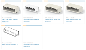
32 position header connector options:
| Connector Part # | Manufacturer Page | Availaility | Sourcing |
|---|---|---|---|
| Desoldered Nissan | ? | You desoldering it from the inverter. Possible to get part # from TE? | |
| 1318745-2 | https://www.te.com/en/product-1318745-2.html | High | https://octopart.com/search?q=1318745-2 |
| 2326784-2 | https://www.te.com/usa-en/product-2326784-2.html | Low | https://octopart.com/2326784-2-te+connectivity+%2F+amp-119798073?r=sp |
| 2326784-3 | https://www.te.com/usa-en/product-2326784-3.html | Low | https://octopart.com/2326784-3-te+connectivity-141486898?r=sp |
| 2322737-1 | https://www.te.com/usa-en/product-2322737-1.html | No | https://octopart.com/2322737-1-te+connectivity-141486892?r=sp |
| 2326784-1 | https://www.te.com/usa-en/product-2326784-1.html | No | https://octopart.com/2326784-1-te+connectivity+%2F+amp-125203930?r=sp |
| 1318745-4 | https://www.te.com/usa-en/product-1318745-4.html | No | https://octopart.com/1318745-4-te+connectivity+%2F+amp-111145194?r=sp |
| 2326784-4 | https://www.te.com/usa-en/product-2326784-4.html | No | https://octopart.com/search?q=2326784-4 |
Listed in TE's 131874-1 32 position female housing, https://www.te.com/usa-en/product-1318747-1.datasheet.pdf
32 position connector
This connector and harness should not need any modifications.
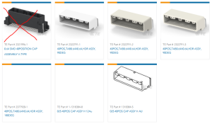
40 position header connector options:
| Connector Part # | Manufacturer Page | Availability | Sourcing |
|---|---|---|---|
| Desoldered Nissan | You desoldering it from the inverter. Possible to get part # from TE? | ||
| 1318384-4 | https://www.te.com/en/product-1318384-4.html | High | https://octopart.com/search?q=1318384-4 |
| 2322791-1 | https://www.te.com/usa-en/product-2322791-1.html | Low | https://octopart.com/2322791-1-te+connectivity+%2F+amp-128564844?r=sp |
| 2322791-2 | https://www.te.com/usa-en/product-2322791-2.html | Low | https://octopart.com/2322791-2-te+connectivity-142686361?r=sp |
| 2322791-3 | https://www.te.com/usa-en/product-2322791-3.html | Low | https://octopart.com/2322791-3-te+connectivity+%2F+amp-119798059?r=sp |
| 2377920-1 | https://www.te.com/usa-en/product-2377920-1.html | No | Not Available? |
| 1-1318384-8 | https://www.te.com/usa-en/product-1-1318384-8.html | No | https://octopart.com/1-1318384-8-te+connectivity+%2F+amp-118490360?r=sp |
| 1318384-5 | https://www.te.com/usa-en/product-1318384-5.html | No | https://octopart.com/1318384-5-te+connectivity+%2F+amp-111145192?r=sp |
Listed in TE's 1318389-1 40 position female housing, https://www.te.com/usa-en/product-1318389-1.datasheet.pdf
40 position Leaf female connector modifications
If you are using the factory Leaf 40 position connector there are many open inverter specific wires that need to be added.
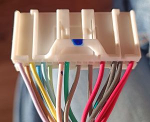
**add which pin numbers or mark them somehow in the table below**

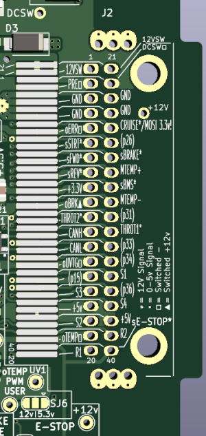
40 position connector pin out:
The 40 position female housing has the following known part numbers:
| Part # | Manufacturer Link | Sourcing | Found Where? |
|---|---|---|---|
| 1318389-1 | https://www.te.com/usa-en/product-1318389-1.html | https://octopart.com/1318389-1-te+connectivity-42270477?r=sp | |
| 2325415-1 | https://www.te.com/usa-en/product-2325415-1.html | https://octopart.com/search?q=2325415-1¤cy=USD&specs=0 | Listed as mating with 2322791-1 |
Terminals for the Nissan connectors
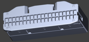
Terminals (female / receptacle) listed to fit the 1318389-1 are here, https://www.te.com/usa-en/product-CAT-T319-T273.html?q=&d=752372&type=products&compatible=1318389-1&samples=N&inStoreWithoutPL=false&instock=N
| Product Description | Marketing Part Number | Products | Terminal Type | Mating Tab Width | Mating Tab Thickness | Terminal Transmits | Wire Size | Wire Size | Sealable | Terminal Seal Type | Wire Size Search |
| CONTACT CRIMP SNAP IN 22-20 | 1-170321-1 | 1-170321-1 | Receptacle | 3 mm | .65 mm | 0 – 24 A (Low Power) | 22 – 20 AWG | .3 – .5 mm² | No | .3 mm², .4 mm², .5 mm² | |
| CONTACT SNAP-IN | 1-170321-4 | 1-170321-4 | Receptacle | 3 mm | .65 mm | 0 – 24 A (Low Power) | 22 – 20 AWG | .3 – .5 mm² | No | .3 mm², .4 mm², .5 mm² | |
| 025 REC CONTACT | 1123343-1 | 1123343-1 | Receptacle | .64 mm | .64 mm | 0 – 24 A (Low Power) | 24 – 20 AWG | .22 – .56 mm² | No | .2 mm², .25 mm², .3 mm², .4 mm², .5 mm² | |
| 025 REC CONTACT GOLD FORMING | 1123343-2 | 1123343-2 | Receptacle | .64 mm | .64 mm | 0 – 24 A (Low Power) | 24 – 20 AWG | .22 – .56 mm² | No | .2 mm², .25 mm², .3 mm², .4 mm², .5 mm² | |
| 025 REC CONTACT PRETIN L/P CUT | 1318143-1 | 1318143-1 | Receptacle | .64 mm | .64 mm | 0 – 24 A (Low Power) | 22 – 20 AWG | .37 – .56 mm² | No | .35 mm², .4 mm², .5 mm² | |
| .025 SEALED REC CONT | 1318329-1 | 1318329-1 | Receptacle | .64 mm | .64 mm | 0 – 24 A (Low Power) | 20 – 18 AWG | .5 – .85 mm² | No | .5 mm², .6 mm², .75 mm² | |
| .040 SEALED REC CONT | 1318332-1 | 1318332-1 | Receptacle | .64 mm | .64 mm | 0 – 24 A (Low Power) | 18 – 16 AWG | .75 – 1.25 mm² | No | .75 mm², 1 mm², 1.25 mm² | |
| 025 IDC REC CONT FORM | 1318688-1 | 1318688-1 | Receptacle | .64 mm | .64 mm | 0 – 24 A (Low Power) | 22 – 20 AWG | .3 – .5 mm² | No | .3 mm², .4 mm², .5 mm² | |
| 025 RCPT IDC TIN (0.08SQ) | 1565403-1 | 1565403-1 | Receptacle | .64 mm | .64 mm | 22 – 20 AWG | .3 – .5 mm² | No | .3 mm², .4 mm², .5 mm² | ||
| 0.64 RCPT SEALED TIN STRIP | 1612290-1 | 1612290-1 | Receptacle | .64 mm | .64 mm | 0 – 24 A (Low Power) | 24 – 22 AWG | .22 – .35 mm² | Yes | Single Wire Seal (SWS) | .2 mm², .25 mm², .3 mm² |
| 0.64 RCPT SEALED AU STRIP | 1612290-2 | 1612290-2 | Receptacle | .64 mm | .64 mm | 0 – 24 A (Low Power) | 24 – 22 AWG | .22 – .35 mm² | Yes | Single Wire Seal (SWS) | .2 mm², .25 mm², .3 mm² |
| REC CONT ASSY S RANGE 025 CLEA | 1717148-1 | 1717148-1 | Receptacle | .64 mm | .64 mm | 0 – 24 A (Low Power) | 22 – 20 AWG | .3 – .5 mm² | Yes | Family Seal | .3 mm², .4 mm², .5 mm² |
| 025 RECEPTACLE CONTACT | 1801069-2 | 1801069-2 | Receptacle | .64 mm | .64 mm | 0 – 24 A (Low Power) | 22 – 20 AWG | .37 – .56 mm² | No | .35 mm², .4 mm², .5 mm² | |
| 025 RECEPTACLE CONTACT | 1801248-2 | 1801248-2 | Receptacle | .64 mm | .64 mm | 0 – 24 A (Low Power) | 20 – 18 AWG | .5 – .75 mm² | No | .5 mm², .6 mm², .75 mm² | |
| 025 RECEPTACLE CONTACT | 2005097-1 | 2005097-1 | Receptacle | .64 mm | .64 mm | 0 – 24 A (Low Power) | 26 – 24 AWG | .13 – .22 mm² | No | .13 mm², .15 mm², .2 mm² | |
| 0.64 RCPT SEALED TIN STRIP(L SIZE) | 2040168-1 | 2040168-1 | Receptacle | .64 mm | .64 mm | 0 – 24 A (Low Power) | 20 AWG | .5 mm² | Yes | Family Seal | .5 mm² |
| 0.64 RCPT SEALED AU STRIP(L SIZE) | 2040168-2 | 2040168-2 | Receptacle | .64 mm | .64 mm | 0 – 24 A (Low Power) | 20 AWG | .5 mm² | Yes | Family Seal | .5 mm² |
**add crimper options**
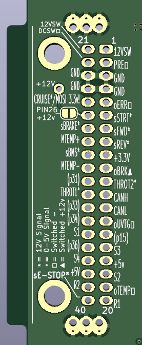
The adapter board is labeled at the 40 position connector to help with wiring up the inverter / harness. Images of these are to the right and a table is below with the positions in order.
The surface mount version of this connector starts with position 21, then 1, 22, 2, etc. The position labeling on the pc board is offset slightly on both sides to help with this.
The pc board renderings / pin labeling images to the right can be used to help populate the connector and wire the vehicle.
| Pos. | Abbreviation | Description | AKA | Details | Pos. | Abbreviation | Description | AKA | Details | |
|---|---|---|---|---|---|---|---|---|---|---|
| 1 | +12VSW | Switched +12v | 21 | +12VSW | Switched +12v | |||||
| 2 | PRE□ | Precharge contactor switched ground | 4.5 ampterminal limit?
recommended to use an economizer |
22 | DCSW□ | EV battery contactor switched ground | 4.5 ampterminal limit?
recommended to use an economizer | |||
| 3 | GND | Ground | 23 | GND | Ground | |||||
| 4 | GND | Ground | 24 | GND | Ground | |||||
| 5 | oERR□ | Output - Error signal, switched ground | 1 amp | 25 | CRUISE*/MOSI3.3v! | Cruise control signal 12v / MOSI 3.3v | 12v set as cruise. 3.3v as MOSI | |||
| 6 | sSTRT* | Input, 12v start signal pulse | 26 | empty / optional +12v | empty - optional +12v for E-Stop switch | See p26 +12V solder jumper notes. | ||||
| 7 | sFWD* | Input, 12v forward | 27 | sBRAKE* | Brake light input 12v | |||||
| 8 | sREV* | Input, 12v reverse | 28 | MTEMP+ | Motor temp senor + | |||||
| 9 | +3.3V | +3.3V from U2 regulator. | Alternative voltage for analog throttles if 5v goes out of range. | 29 | sBMS* | Battery Management System error +12 signal | ||||
| 10 | oBRK▲ | Output, brake +12v (see SJ4) | 1.5 amps | 30 | MTEMP- | Motor temp sensor - | ||||
| 11 | THROT2° | Throttle 2, 0-5v signal | 5K pull down to gnd on mini mainboard to shift to 0-3.3v. | 31 | empty | empty | ||||
| 12 | CANH | CAN high signal (see SJH1) | 120 ohm termination resistor solder jumpers | 32 | THROT1° | Throttle 1, 0-5v signal | 5K pull down to gnd on mini mainboard to shift to 0-3.3v. | |||
| 13 | CANL | CAN low signal (see SJL1) | 120 ohm termination resistor solder jumpers | 33 | empty | empty | ||||
| 14 | oUVTG□ | optional output? 1amp max switched ground | 1 amp | 34 | empty | empty | ||||
| 15 | empty | empty | 35 | S1 | Encoder S1 wire | |||||
| 16 | S3 | Encoder S3 wire | 36 | empty | empty | |||||
| 17 | +5V | +5V for sensors (like throttle) | 37 | S4 | Encoder S4 wire | |||||
| 18 | S2 | Encoder S2 wire | 38 | +5V | +5V for sensors (like throttle) | |||||
| 19 | oTEMP□ | over temp signal, switched ground, 1 amp max | 1 amp, has EMI filter capacitor (C11) for PWM | 39 | R2 | Encoder R2 wire | ||||
| 20 | R1 | Encoder R1 wire | 40 | sE-STOP | Optional Emergency stop switch (see SJ5) | Can add an E-Stop switch to 12v. |
| KEY |
| * = 12v Signal |
| ° - 0-6.6v Signal |
| □ = Switched ground |
| ▲ = Switched +12v |
A visual pin numbering of the 40 position connector.
Programming the ESP32 Wi-Fi module

Solder jumper JP8 & J8 set the programming header voltage to either 5v or 3.3v. Use only 1 header to set the voltage to your programmer's output voltage.
If 5v is used the 3.3v regulator will convert it to 3.3v for the ESP32.
J4 is used to program the ESP32.
There is a slot above the labels 38 and J4 for a zip tie hole to hold an antenna wire. This can be used if a u.FL antenna is used along with an ESP32-S2-Wroom-I module.
| Position | Description |
|---|---|
| 1 | IO0 |
| 2 | GND |
| 3 | GND |
| 4 | +3.3v / +5V, (J8 / JP8) |
| 5 | ESP32 USART_RX |
| 6 | ESP32 USART_TX |
Note that the enable line is broken out on the other side of the ESP32 if needed.
R25 and C13 are for boot delay to assist programming.
Follow instructions here Esp32-web-interface
**add info about programming with the STM32 processor programmed already**
**add info about the boot delay** ESP32 boot delay R & C is set to the commonly recommended 10k resistor & 1uF in V0.0.1. V0.0.4 swapped back to 4k7 / .1uF because the esp32 recommended boot delay values caused issues in the STM32 booting properly
switch back.
Programming the STM32
Add info on programming the STM32 processor.
Currently the recommendation is to program the ESP32 first, then the STM32.
**settings info** link..
**Editing the IP address if using multiple motors.**
**options** link..
Extra header J3
**add info about the extra header** what's the use case?
J3 gives access to TX & RX lines to the STM32 along with 3.3v and ground if the ESP32 is not populated. J3 is labeled from the ESP32.
C19 is an unpopulated handsolder 0805 capacitor footprint if this optional header is used and 3.3V power dips. There is also an unpopulated 10x10.5 aluminum capacitor footprint at C20 to assist even more if needed.
| Position | Description |
|---|---|
| 1 | +3.3v |
| 2 | GND |
| 3 | STM32 USART_TX |
| 4 | STM32 USART_RX |
| 5 | empty |
| 6 | empty |
| 7 | empty |
| 8 | empty |
| 9 | empty |
| 10 | empty |
Contactor outputs, PRE & DCSW
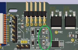
**4.5 amps max (header terminal limited?, otherwise 10-17A max to be determined with testing.)** These need to be tested both for current and heat issues.
**add economizer circuit if not included in contactor**
**There are unpopulated 0805 capacitor footprints on each contactor gate, these are optional to help eliminate chatter if required. Required? Contactor chatter issues?** too much will make the mosfet stay in the linear region for a while, could damage them.
Brake output
There is a high side switch soldered on the board that outputs +12v @ 1.5A maximum when regen is active. This is likely not enough to drive brake lights directly. It is up to the user to combine the vehicles brake switch output with this brake output +12v signal. Consider an automotive SSR with the vehicles normal brake output feed through a diode along with the inverter brake output through a diode so either or both turn on the SSR.